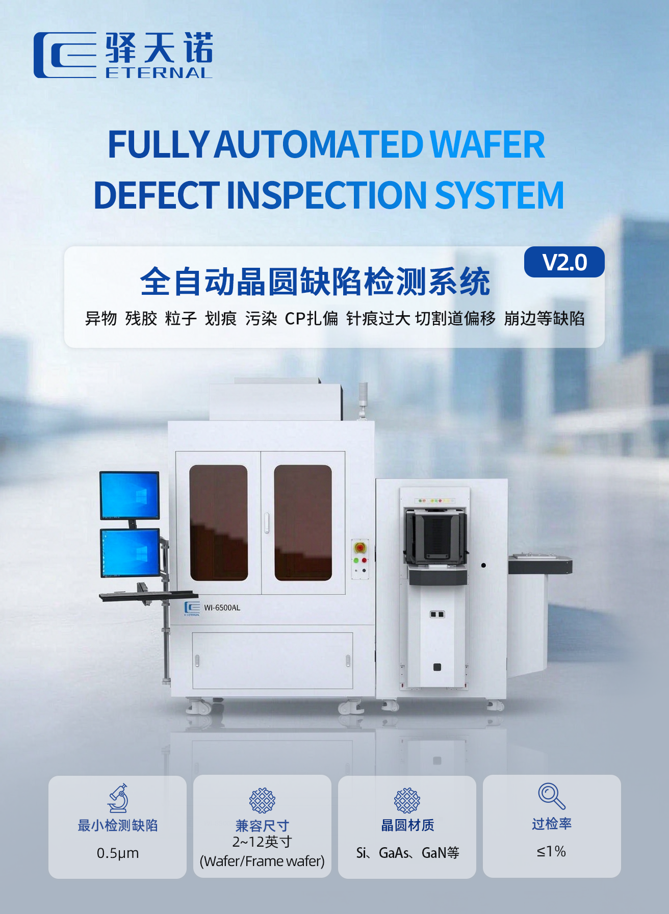
The 2.0 version of the WI-6500AL Fully Automated Wafer Defect Inspection System has been officially launched. It consists of an automated loading and unloading system, a visual inspection system, and control software, and supports automatic defect detection for 25-wafer and frame-wafer configurations.
The system has been fully upgraded to integrate with a large AI model, endowing it with machine learning and self-iteration capabilities. This significant enhancement has notably improved the accuracy of defect recognition, significantly reducing false positives and missed detections. Additionally, a new flying scan and line scan mode has been introduced, enabling precise and continuous imaging during high-speed motion, significantly increasing detection throughput and easily meeting the demands of high-capacity production lines. The system can still quickly detect the number and position of wafers, accurately locate defects, intelligently identify types, and store data in real-time in a database. It is suitable for inline and downstream processes, comprehensively improving accuracy, efficiency, and stability, thus ensuring the quality of wafers.
01 Integrated with a large AI model, equipped with machine learning capabilities
Integrating a large AI model is akin to equipping traditional automatic optical inspection equipment with a "smart brain" capable of self-learning and evolution. This fundamentally alters the way the equipment detects and identifies defects, transitioning from "passive comparison" to "active learning", thereby safeguarding wafer yield with its continuously evolving capabilities
02 Flying scanning with line scanning significantly enhances detection efficiency
Flying scanning provides speed, while line scanning ensures accuracy. It guarantees that each scanned image line can be accurately stitched, ultimately generating a complete wafer image with high resolution and no distortion, significantly improving detection efficiency while maintaining accuracy.
Minimum defect size of 0.5μm (supporting both brightfield and darkfield observation)
Wafer size: 2~12 inches (wafer/Frame wafer)
Automated loading and unloading, with a test capacity of 25 pieces per batch
Automatic detection by machine vision system
Autofocus and layered focus image capture
Defect analysis, generate Map report
MAIN FUNCTIONNAL PARAMETERS
| Compatible Wafer Sizes | Compatible Wafer Sizes: 2~12 inches (customizable); supports blue film, chip adsorption boxes, and other formats |
| Wafer material | Si、GaAs、GaN |
| Imaging Type | Color/Monochrome |
| Magnification | 1.25X/2.5X/5X/10X/20X/50X (etc.) |
| Defect Detection | Automated |
| Defect Types | Contamination, waveguide fractures, scratches, color anomalies, pin mark deviations, silicon cracks, edge chipping, etc. |
| Defect Detection Error Rate | 0.1% |
| Minimum Detection Resolution | 0.5μm |
| Cassette Capacity | 1~2 cassettes |
WI-6500AL Fully Automated Wafer Defect Inspection System is the core equipment for yield control in semiconductor manufacturing, and its core advantages are mainly reflected in dimensions such as high precision, high efficiency, intelligence, deep data value, and good stability.
Wafer defect detection is a crucial part of the packaging and testing process, and Eternal has always been committed to providing more accurate, efficient, and intelligent detection solutions to safeguard every wafer.
ETERNAL welcomes inquiries about cooperation
WI-6500AL Fully Automated Wafer Defect Inspection System 2.0 are available for consultation and customization
Contact us for detailed technical specifications or to arrange a product demonstration